Project Overview
I developed this jig to automate the testing of complex PCBs.
Key Components
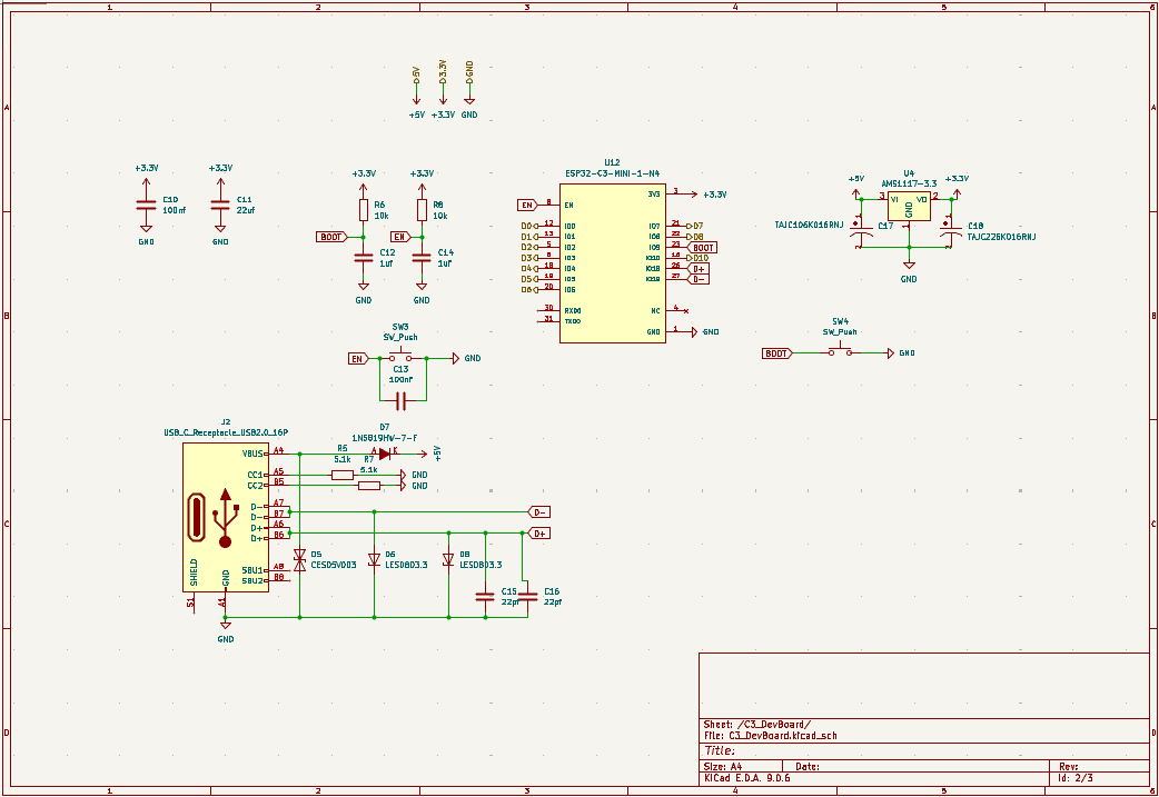
- Microcontroller Dev Board: ESP32-C3-MINI.
- Hardware: Pogo pins and custom 3D-printed alignment frame.
- Software: Python-based data logging.
Design Process
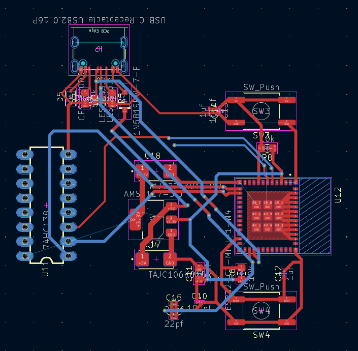
I used KiCad for the schematic capture and PCB layout, focusing on a stackup that ensures signal integrity.
C3 DEV Board Design
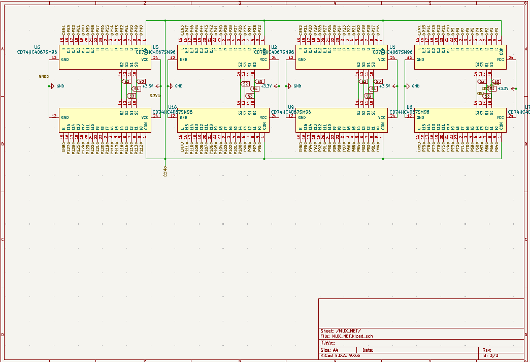
MUX Network to Visualize the Nets
C3 DEV Board PCB Layout